 Open Access



 Open access
 Check for updates

Abstract
The geometric structure of graphene under an external electric field was investigated using the density functional theory (DFT). DFT calculations revealed that the hole injection into graphene highly modulates the geometric structure of graphene. The lattice parameter of graphene monotonically increased with increasing the hole doping concentration. The lattice constant is insensitive to the electron doping. The fragility and robustness against the hole and electron doping, respectively, are ascribed to the electronic structure of graphene under the electric field. The wave function analysis revealed that the holes are accommodated in the bonding π states, weakening covalent bonds between C atoms. In contrast, the electrons are primarily accommodated in nearly free electron states with a maximum amplitude above and below the graphene layer.
Introduction
Since its discovery, graphene has attracted scientific and technological interest due to its excellent physical properties resulting from its honeycomb covalent network of C atoms with atom thickness [1],[2]. The honeycomb covalent network of sp2 C atoms gives graphene high chemical stability, remarkable mechanical stiffness, and out-of-plane flexibility [3]-[5]. In addition to these structural properties, the itinerant electrons on the honeycomb network led to the unique electronic structure at and around the Fermi level and the K point in the hexagonal Brillouin zone [6],[7]. Graphene possesses conical dispersion bands at the Fermi level that cause the remarkable carrier mobility of 200000 cm2/Vs or more [8],[9]. Therefore, graphene is regarded as an emerging material for fabricating functional devices in wide fields of modern technologies. In addition to those properties of isolated graphene, graphene is considered a building block of various complexes by stacking with the other graphene layers and other atomic layer materials, such as hBN and transition-metal dichalcogenide [10],[11]. These complexes show further unique physical properties that exceed the simple superposition of physical properties of constituent layers [12]-[13]. The conical dispersion band of graphene is fragile by forming a heterostructure with hBN [13]. More interestingly, bilayer graphene shows unique variations in their electronic structures, which are sensitive to their interlayer stacking arrangement [14],[15]. An external electric field or excess carriers on graphene and its derivatives is another essential control parameter of their physical properties. In the case of bilayer graphene with AB stacking arrangement and thin films with ABC stacking arrangement, a perpendicular electric field can create a finite band gap whose width depends on the field strength [16]-[19]. Furthermore, the field or excess carrier can control the Fermi energy of graphene concerning the Dirac point, increasing the current density throughout the channel of the field effect devices. These facts indicate that the electric field is decisive in determining the electronic properties of graphene and its complexes. Despite these physical insights into the field effect on electronic properties, the field effect on the structural properties of graphene is still unclear. This knowledge is crucial for practical applications of graphene because the electronic properties of graphene and its derivatives are sensitive to their geometries. Therefore, this paper aims to clarify the geometric structure of graphene with excess carriers, which are injected by the external electric field, using the density functional theory combined with the effective screening medium method.
Calculation Method
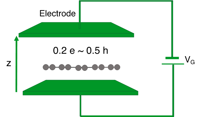
All calculations are performed in the framework of density functional theory (DFT) implemented in the Simulation Tool for Atom TEchnology (STATE) program package [20],[21]. The exchange-correlation potential energy between the interacting electrons is expressed using the generalized gradient approximation with a Perdew-Burke-Ernzerhof functional [22]. Interaction between the valance electrons and ions is treated using an ultrasoft pseudopotential generated by the Vanderbilt scheme [23]. To inject electrons or holes into graphene implemented in field effect transistors, we used the effective screening medium method, which allowed us to directly simulate the graphene field effect transistor with a dual gate electrode simulated by the effective screening medium with infinite permittivity (Fig. 1) [24]. The gate electrodes are situated above and below the graphene layer with 5 Å vacuum spacing. Here, we investigate the geometric structure of graphene under the carrier concentrations of 0.2 e/cell ~ 0.5 h/cell. Integration over the Brillouin zone was carried out using an equidistance mesh of 21x 21x1 k points.
Result and discussion
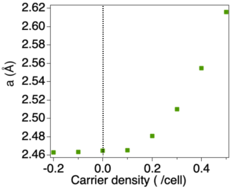
Figure 2 shows the lattice parameter of monolayer graphene under excess carriers by the external gate voltages. The lattice parameter shows a different characteristic after injecting the excess electrons and holes. The lattice parameter increases with the increase in hole density. The lattice parameter is 2.61 Å under the hole doping concentration of 0.5h/cell, which is longer by 0.15 Å than that under the neutral condition (2.46 Å). Therefore, the chemical bonds of graphene are fragile against hole injection. In contrast, the lattice parameter of graphene is robust against electron doping. The lattice parameter retains that of the neutral value under the electron concentrations of 0.1 and 0.2 e/cell.
We investigated the electronic structure of graphene with excess carriers to provide the physical mechanism of the lattice parameter modulation of graphene. Figure 3(a) shows the electronic structures and squared wave function of the Dirac point at the K point and the lowest branch of the conduction at the Γ point of monolayer graphene without excess carriers. The wave function associated with the Dirac point is distributed throughout the graphene layer with π state nature. The wave function associated with the lowest branch of the conduction band at the Γ point has a unique distribution. The wave function is distributed not only on the C atomic layer but also in the vacuum spacing outside the layer known to be nearly free electron (NFE) states [7]. The carrier injection highly modulates the electronic structure of graphene. For the electron doping, the parabolic band at the Γ point substantially shifts downward and crosses the Fermi level, indicating the carrier injection into this NFE state. While the Dirac point at the K point is still located at the Fermi level (Fig. 3(b)). Thus, the injected electrons are primarily accommodated in the NFE states and do not affect the chemical bond of graphene. In contrast, the Fermi level substantially shifts downward under the hole injection into the graphene, clearly indicating that the electron density of the bonding π states decreases by the hole injection (Fig. 3(c)). Thus, the covalent bond between C atoms is weakened, increasing the lattice parameter.
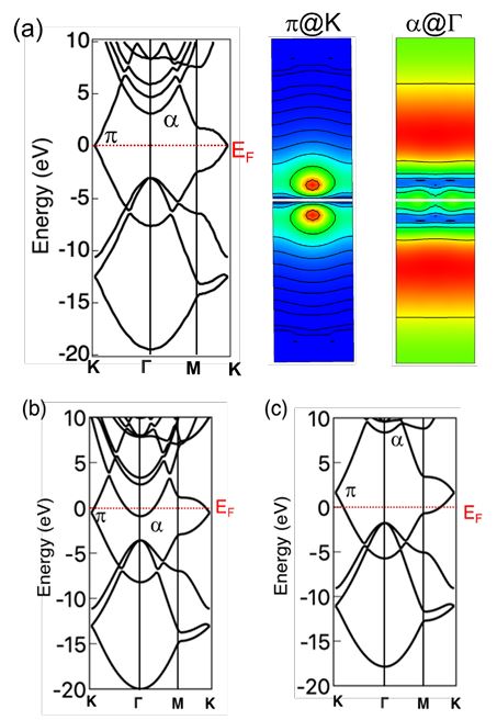
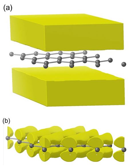
Figure 4 shows the electron and hole distribution in graphene under an electron doping concentration of 0.2e/cell and hole doping concentration of 0.2h/cell, respectively, by the corresponding gate voltage. The accumulated electron is not distributed on the graphene layer but in the vacuum spacing above the graphene layer. The distribution corroborated that electron doping does not affect the covalent bond of graphene. In contrast, the accumulated holes have a distribution that is the same as that of the π electron states of graphene. Thus, the electron density on bonding π states decreases by the hole doping. This electron density decrease may weaken the covalency of the honeycomb network of graphene and increase the lattice parameter with increasing the hole concentration.
Summary
We studied the geometric structure of graphene under the excess electrons and holes that are injected by the gate electric field in terms of the doping concentration based on density functional theory with the effective screening medium method. Our analysis revealed that the geometric structure of monolayer graphene is sensitive to hole doping, leading to the fact that the lattice parameter monotonically increases with increasing the hole concentration. In contrast, the geometric structure of graphene is insensitive to electron doping. The lattice parameter of graphene retains its value up to the electron concentration of 0.2e/cell. The fragility and robustness against the carrier injection are ascribed to the electronic structure of graphene with excess carriers. The electron doping causes a substantial downward shift of the NFE state, which is distributed not only on the atomic layer but also in the vacuum spacing. Accordingly, the electrons are primarily accumulated in this NFE state while they do not affect the π electron states. Therefore, the covalent bond is insensitive to the electron concentration. In contrast, the holes are accommodated in bonding π states. Thus, the hole doping weakens the covalent bonds, and the lattice parameter increases with the increase of the hole concentration.
<div><br></div><div>Ethical Approval</div>
The submitted work is a unique contribution to the field, not published elsewhere in any form or language. Results are presented clearly, honestly, and without fabrication, falsification or inappropriate data manipulation (including image-based manipulation). Authors adhere to discipline-specific rules for acquiring, selecting and processing data.
Consent of Participate
The submitted work is theoretical work on atomic layer materials. No human subject or living organism/tissue is involved in this research.
Consent to Publish
No consent to publish is to be shared.
Declarations
- Author contributions
All authors contributed to the study conception and design. Design and analysis were performed by Nadia Sultana. The first draft of the manuscript was written by Nadia Sultana and all authors commented on previous versions of the manuscript. All authors read and approved the final manuscript.
- Funding
The authors are grateful to the Japan Science and Technology Agency under JST-CREST grant number JPMJCR20B5 and JPMJCR23A4, the Japan Society for the Promotion of Science under JSPS KAKENHI grant numbers JP23H05469, JP22H00283, JP21H05232, JP21H05233, JP21K14484, and JP20H05664, and the Joint Research Program on Zero-Emission Energy Research, Institute of Advanced Energy, Kyoto University.
- Data availability
Not applicable
- Competing interests
Not applicable
References
- 1.Dresselhaus, M. S., and Dresselhaus, G., (1981). Intercalation compounds of graphite. Advances in Physics, 30(2): 139-326.
- 2.Castro Neto, A. H., Guinea, F., Peres, N. M., Novoselov, K. S., and Geim, A. K., (2009). The electronic properties of graphene. Reviews of Modern Physics, 81(1): 109-162.
- 3.Geim, A. K., and Novoselov, K. S., (2007). The rise of graphene. Nature Materials, 6(3): 183-191.
- 4.Zhang, Y., Tang, T. T., Girit, C., Hao, Z., Martin, M. C., Zettl, A., Crommie, M. F., Shen, Y. R., and Wang, F., (2009). Direct observation of a widely tunable bandgap in bilayer graphene. Nature, 459(7248): 820-823.
- 5.Ghosh, S., Nika, D. L., Pokatilov, E. P., and Balandin, A. A., (2009). Heat conduction in graphene: experimental study and theoretical interpretation. New Journal of Physics, 11(9): 095012.
- 6.Painter, G. S., and Ellis, D. E., (1970). Electronic band structure and optical properties of graphite from a variational approach. Physical Review B, 1(12): 4747.
- 7.Posternak, M., Baldereschi, A., Freeman, A. J., Wimmer, E., and Weinert, M., (1983). Prediction of electronic interlayer states in graphite and reinterpretation of alkali bands in graphite intercalation compounds. Physical Review Letters, 50(10): 761-764.
- 8.Zhang, Y., Tan, Y. W., Stormer, H. L., and Kim, P., (2005). Experimental observation of the quantum Hall effect and Berry's phase in graphene. Nature, 438(7065): 201-204.
- 9.Bolotin, K. I., Sikes, K. J., Jiang, Z., Klima, M., Fudenberg, G., Hone, J., Kim, P., and Stormer, H. L., (2008). Ultrahigh electron mobility in suspended graphene. Solid State Communications, 146(9-10): 351-355.
- 10.Geim, A. K., & Grigorieva, I. V., (2013). Van der Waals heterostructures. Nature, 499(7459): 419-425.
- 11.Ago, H., Okada, S., Miyata, Y., Matsuda, K., Koshino, M., Ueno, K., and Nagashio, K., (2022). Science of 2.5 dimensional materials: paradigm shift of materials science toward future social innovation. Science and Technology of Advanced Materials, 23(1): 275-299.
- 12.Maruyama, M., Nagashio, K., and Okada, S., (2020). Carrier Distribution Control in van der Waals Heterostructures of MoS2 and WS2 by Field-Induced Band-Edge Engineering. Physical Review Applied, 14(4): 044028.
- 13.Okada, S., (2010). Semiconducting electronic structure of graphene adsorbed on insulating substrate: fragility of the graphene linear dispersion band. Japanese Journal of Applied Physics, 49(2R):020204.
- 14.Koshino, M., and Ando, T., (2007). Orbital diamagnetism in multilayer graphenes: Systematic study with the effective mass approximation. Physical Review B, 76(8): 085425.
- 15.Koshino, M., and Ando, T., (2008). Magneto-optical properties of multilayer graphene. Physical Review B, 77(11): 115313.
- 16.Otani, M., and Okada, S., (2010). Field-induced free-electron carriers in graphite. Journal of the Physical Society of Japan, 79(7): 073701.
- 17.Oostinga, J. B., Heersche, H. B., Liu, X., Morpurgo, A. F., and Vandersypen, L. M., (2008). Gate-induced insulating state in bilayer graphene devices. Nature Materials, 7(2): 151-157.
- 18.Gao, Y., and Okada, S., (2021). Carrier distribution control in bilayer graphene under a perpendicular electric field by interlayer stacking arrangements. Applied Physics Express, 14(3): 035001.
- 19.Sultana, N., Maruyama, M., Gao, Y., and Okada, S. (2023). Electronic structure of graphene thin films under a perpendicular electric field. Japanese Journal of Applied Physics, 62(7): 075001.
- 20.Kohn, W., and Sham, L. J., (1965). Self-consistent equations including exchange and correlation effects. Physical Review, 140(4A): A1133.
- 21.Morikawa, Y., Iwata, K., and Terakura, K., (2001). Theoretical study of hydrogenation process of formate on clean and Zn deposited Cu (1 1 1) surfaces. Applied Surface Science, 169:11-15.
- 22.Perdew, J. P., Burke, K., and Ernzerhof, M. (1996). Generalized gradient approximation made simple. Physical Review Letters, 77(18): 3865.
- 23.Vanderbilt, D., (1990). Soft self-consistent pseudopotentials in a generalized eigenvalue formalism. Physical Review B, 41(11): 7892-7895.
- 24.Otani, M., and Sugino, O., (2006). First-principles calculations of charged surfaces and interfaces: A plane-wave nonrepeated slab approach. Physical Review B, 73(11): 115407.
Cite this article
Journal
Sultana N, Gao Y, Maruyama M, Okada S. Structural modulation of graphene by an external electric field. JoSEP. 2026;2(1):101-104. doi: 10.62275/josep.25.1000015.
Rights and permissions
© 2026
Cited by (0)
Citing works are not available yet.
About this article
- Received
- 30 September 2024
- Revised
- 6 November 2024
- Accepted
- 12 November 2024
- Published
- 21 October 2026
- Journal
- Journal of Science and Engineering Papers
- Volume / Issue
- 2 / 1
- Pages
- 101-104
- DOI
- 10.62275/josep.25.1000015